I noticed recently that I’m spending too much time building boards – it seems that my trusty air rework station just can’t work any harder. With ski season just a week away, I was looking at ways to minimize any work-related activity to save energy for skiing. As luck would have it, weather this weekend was extremely unpleasant – perfect time to stay home and upgrade my production to small scale plastic stencil/toaster oven process pioneered by Sparkfun and improved by many others. Below is my experience with it together with some pictures – enjoy!
In addition to typical household equipment – old decommissioned toaster oven, putty knife, paper towel, rubbing alcohol, and pair of good tweezers the process calls for two special items, which would have to be ordered in advance. One of it is a solder paste, another is a stencil to apply solder paste over PCB pads.
A Gerber for a stencil can be made from tCream layer in Eagle. This layer is generated automatically and works as-is with no modifications in most cases. However, if board contains packages with power pads, default footprint needs to be modified. Screaming Circuits has an article about proper QFN power pad solder paste pattern.
The stencil itself can be made from several different materials. Large scale production shops use stainless steel. Stainless steel stencil can be cut very precisely and work for many application cycles; it is, however, expensive. Another popular material is Mylar; it is not very durable but cheap. Kapton is more sturdy than Mylar (NASA used it as a micrometeoroid protection layer in space suits for Moon mission and Skylab project) and cost is roughly the same as Mylar – I prefer this material for my stencils.
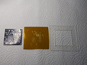
| I ordered my Kapton stencil from Ohararp. Picture on the right shows the stencil, a PCB holder, as well as PCB for which it was made, my USB Isolator) design. The stencil is very well cut, aligns easily thanks to it’s color, and doesn’t show any signs of deterioration after numerous printings and cleanings. The holder is extremely useful, it saves a lot of setup time and desk space. The setup is very simple – place PCB in holder, place stencil on top, align and affix to one side with a piece of scotch tape. After that stencil can be used, cleaned and stored time after time without reattaching and realigning. | |
|
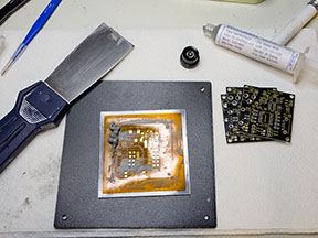
Let’s do some printing. I never tried to use any fancy squeegees built for the purpose. Other people’s posts on the topic suggest that any piece of rigid material with straight edge will work. From what I have at hand, putty knife works best.
The paste that I use is Amtech Syntech-LF – synthetic-based paste with outstanding properties. Note the expiration date on the syringe – still feels fresh. Also, since this paste is less sensitive to ambient temperature, suppliers won’t insist on overnight shipping in cold pack when I buy it. |
|
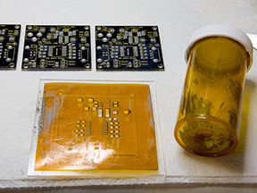
| This is how stencil looks when paste is applied. For this particular PCB I don’t scrape it clean; large 1206 resistor/capacitor packages and tantalum D cases require some extra solder. | |
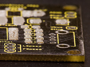
| Take a look at the pad with paste applied. Again, this amount is good for big packages – small ones need thinner layer of paste. | |
| After all boards were printed, I scraped the paste form the stencil and putty knife and placed it in another container. This way paste can be reused; if it becomes dry, it can be mixed with fresh paste from the syringe. | |
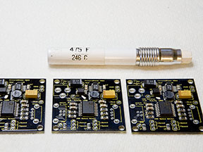
| I populated my boards with old-fashioned “tweezers in hand” process and now they are ready to be toasted. Note little white thing to the left of the inductor on each board. This is temperature marker. It melts and liquefies when it’s reaches correct temperature; very handy during reflow process tuning. | |
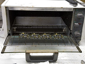
| Obligatory toaster picture. I place boards on a shelf so that temperature marker is visible through the door, slide the shelf in and set toaster to “Bake” at just a hair less than 400F for 5 minutes. After that I crank the temperature up to 500F and watch boards reflow and temperature markers melt. While melting, marker becomes transparent, so it looks like disappearing. When this happens, I open the toaster door (this also turns it off) and let boards to cool off before taking them out. | |
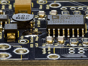
| This is final closeup. Note the result – nice shiny solder joints (it’s lead free solder so they are not really that shiny; I just created the effect with some clever light placement). You can also see how temperature marker looks like after heating. It can be removed by scraping or washed away with IPA. |
As you can see, reflow soldering can be performed quite easily with minimum investment in special tools and materials. It saves time and produces nice uniform joints. Also, it is lot easier than manual soldering using air rework station or soldering iron. If you’d like to try this process and have questions, please ask.
Happy soldering!
Oleg.


[…] This post was mentioned on Twitter by Radio ReTweeter. Radio ReTweeter said: RT @omazurov yet another toaster oven reflow soldering article -> http://bit.ly/bzBob… http://urlwee.com/bUH […]
Thanks for this post. I have been a bit tentative at getting started with this, but you have shown that it can be done easily and relatively cheaply.
[…] that cover using stencils to populate boards and using ovens to reflow. [Oleg] has put together a tutorial on the process he uses to populate and reflow his own […]
Have you tried the skillet method yet. I haven’t tried either but I was thinking that the skillet method was gaining popularity in the DIY community.
I haven’t tried skillet since i don’t own one, however, I don’t think there is a big difference between methods. If you need to buy your soldering device, buy a skillet; it’s easier to tune and you can see better what is going on. On the other hand, if you already have a toaster that can be dedicated to soldering, just use it.
[…] http://www.circuitsathome.com/production/on-reflow-soldering a few seconds ago from web […]
If I may ask, where did you get the Amtech Syntech-LF? I searched all over the internet for it, and can’t seem to find it…
Here’s one place -> http://www.solderandmore.com/servlet/the-No-dsh-Clean-Solder-Paste/Categories . You can also go to Amtech site, find list of reps and call one.
I’ve never seen a temperature marker like that, but I can see where it would be very useful. Where did you buy it from?
@Alan: I use the skillet method and it really is very easy if you’re doing boards that only have components on one side. I’ve never had to do a board with components on both sides, so that’s the option I chose. I’m using an old toastmaster hot plate and a cheap aluminum frying pan. Temperature is controlled by my left hand while I use a contactless IR thermometer to read how hot the skillet is. Just heat to about 235 C, put in the board, and wait for reflow which takes about 2 to 3 minutes.
Signal7 – The marker came from Stencils Unlimited.
Que grande! The best reason that I´ve never hear for to make your work in a more optimal way.. Skiing! I envy you, all the day skiing and, in your free time…design electronics, soldering boards…
Yes, I love exteme skiing and electronics.. and some day I will do the same that you…
Regards from Spain!
Brilliant work! I need to get ahold of that temperature marker 😉
Hallo!
Please, i’m looking for make the serigraphy, i looked yours in yellows, how did you do?
You mean silkscreen on the PCB? I didn’t make it, my boardhouse makes this color on request.